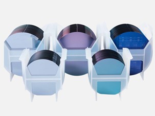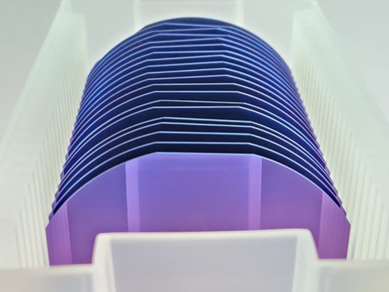
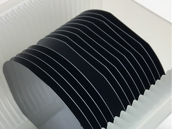
Si/SiO2 Wafer
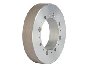
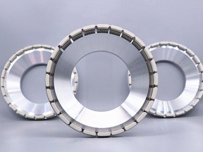
Cylindrical grinding wheel
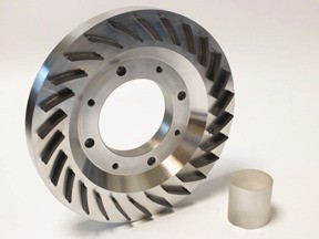
Back grinding wheel
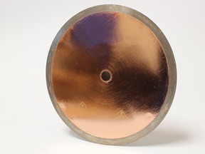
Diamond band saw for cutting sapphire
Diamond edge grinding wheel for sapphire
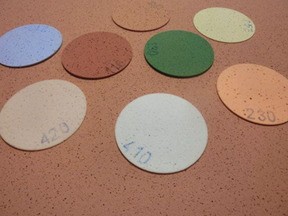
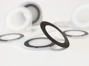
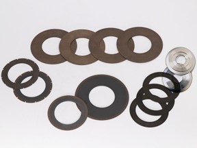
Diamond polishing pate, diamond compound, diamond polishing pad
Silicon oxide wafers use thermal oxidation process, through atmospheric pressure furnace tube equipment at high temperature (800℃~1150℃) conditions, through oxygen or water vapor on the surface of silicon wafer growth of silicon dioxide film. Processing thickness ranges from 50 nanometers to 2 microns, process temperatures up to 1100 degrees Celsius, and growth methods are divided into “wet ” and “dry “. The thermal oxide layer is a kind of oxide layer formed by “growth”. Compared with the oxide layer deposited by CVD, it has higher uniformity, better compactness and higher dielectric strength, and its quality is more excellent.
The thermal oxide layer is an excellent dielectric layer as an insulator. In many silicon-based devices, the thermal oxide layer plays an important role as a doping barrier layer and surface dielectric.
Technical specifications for Si/SiO2 wafers
| Parameter | data |
| Diameter | 50.8±0.38 |
| Grade | Prime |
| Material | Si+Sio2(thermal) |
| Orientation | (100)±0.5℃ |
| Thickness of wafer(μm) | 280±25 |
| Thickness of oxide(thermally grown) | 500±50 |
| Doping | Undoped, intrinsic Si(Fz grown) |
| Polish | Single side polished Si |
| Resistivity(ohm-cm) | >20000 |
| Front surface | Polished |
| Back surface | Etched |
| Packaging | Hard cassette |
| Shelf life | 6 months,min,at the time of delivery |
Technical specifications for N-type Si wafers
| Parameter | data |
| Diameter | 50.8±0.38 |
| Grade | Prime |
| Material | Si+Sio2(thermal) |
| Orientation | (100)±0.5℃ |
| Thickness of wafer(μm) | 280±25 |
| Doping | Undoped, intrinsic Si(Fz grown) |
| Polish | Single side polished Si |
| Resistivity(ohm-cm) | >20000 |
| Front surface | Polished |
| Back surface | Etched |
| Packaging | Hard cassette |
| Shelf life | 6 months,min,at the time of delivery |
Technical specifications for sapphire substrates
| Parameter | |
| Diameter | 50.8±0.20 |
| Material | Al2o3 |
| Purity | 99% or better |
| Crystal | Single crystal |
| Orientation | C-plane,(0001)±0.5° |
| Primary flat length | 16±1mm |
| TTV(μm) | ≤10 |
| BOW(μm) | ≤10 |
| WARP(μm) | ≤10 |
Related Products
-
Back Grinding Wheel for LED Substrate
Back Grinding Wheel for LED Substrate
-
Edge Grinding Wheel, Silicon Wafer Chamfering
Edge Grinding Wheel, Silicon Wafer Chamfering
-
Polyurethane (PU) Polishing Pad for Wafer Surface
Polyurethane (PU) Polishing Pad for Wafer Surface
-
Si/SiO2 Wafer
Si/SiO2 Wafer
-
Back Grinding Wheel for Surface Grinding Various Silicon Wafer
Back Grinding Wheel for Surface Grinding Various Silicon Wafer
-
Resin Diamond Dicing Blade for Silicon Wafer
Resin Diamond Dicing Blade for Silicon Wafer
-
Diamond Dicing Blades For Wafer Scribing
Diamond Dicing Blades For Wafer Scribing
-
Metal bond diamond cutting wheel , steel core with copper plated is used for grooving and cutting carbide,optics glass, sapphire, ceramics , magnetic materials and semiconductor material
Metal Diamond Wafer Blade with Copper Plated
Please Feel free to give your inquiry in the form below. We will reply you in 24 hours.

